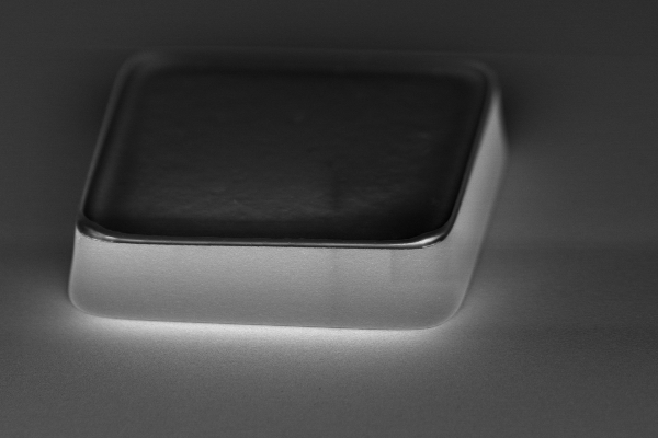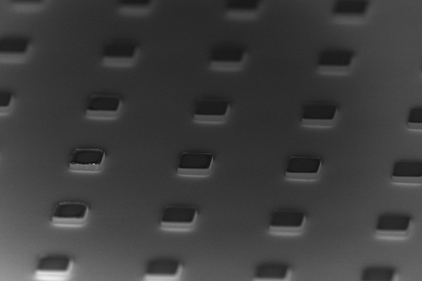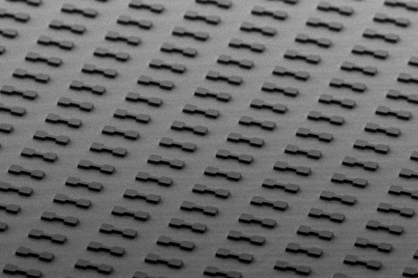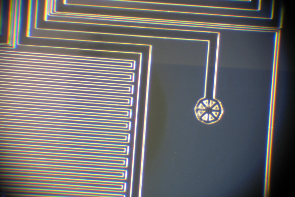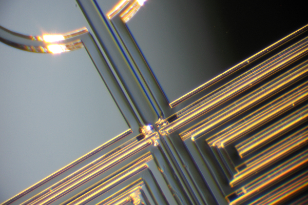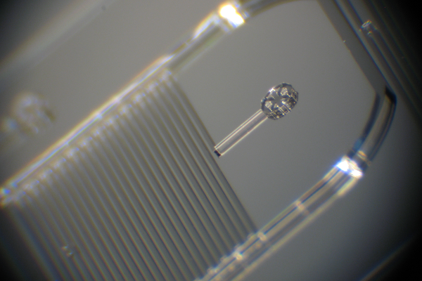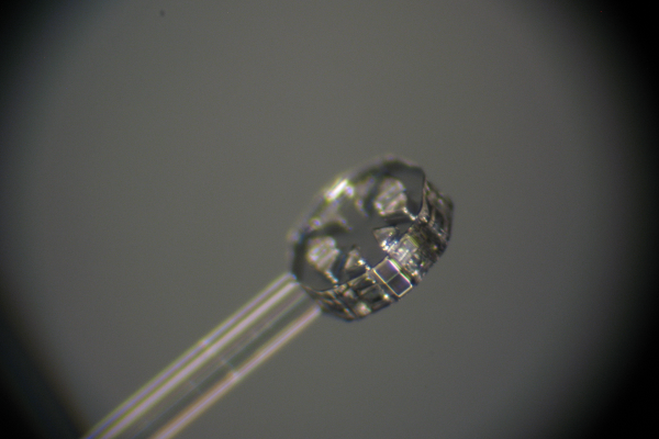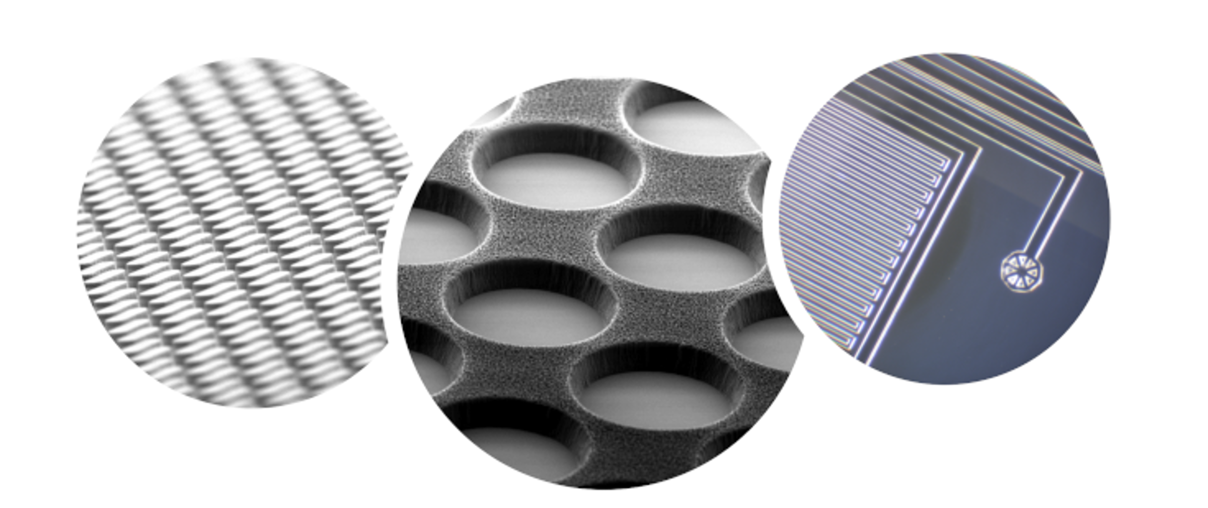
We fabricate artificially designed micro-environments to culture and probe living cells. Arrays of defined cavities provide standardized geometric boundaries for individual cells or groups of cells. We study single cell gene expression, cell migration and apoptotic events with precise spatio-temporal control. To this end we develop biofabrication techniques, including photo-lithography, hot-embossing, electroplating, soft lithography, 3D printing and microcontact printing, to create two-dimensional (2D) and three-dimensional (3D) pattern, cavities and channels made of biocompatible materials like PDMS, COC, hydrogels and proteins. The 3D microenvironments allow for long-term observation of growth and function of individual living cells, interacting groups of cells and organoids.
Lithography
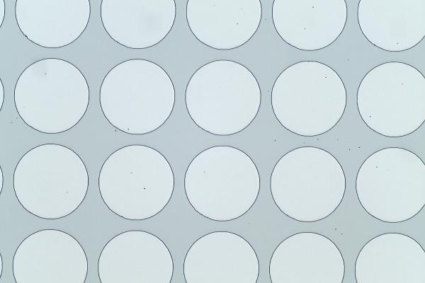
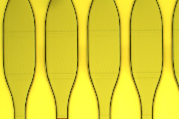
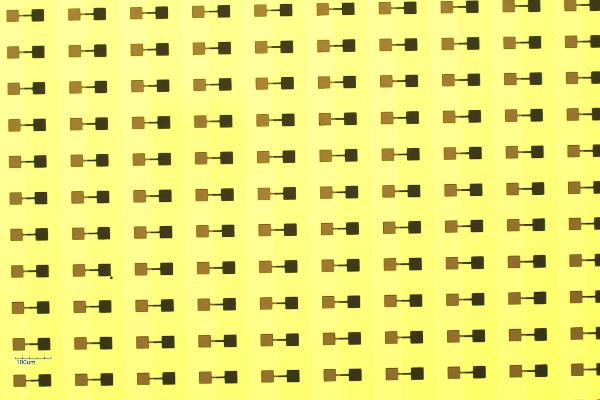
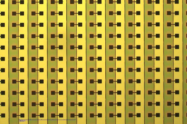
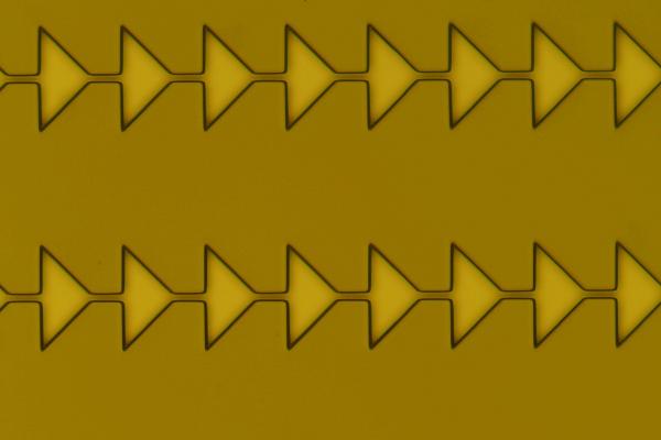
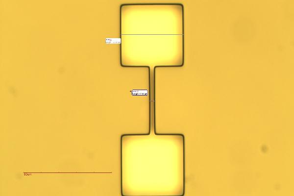
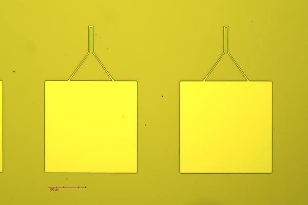
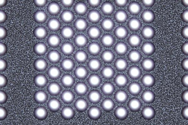
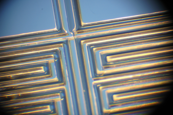
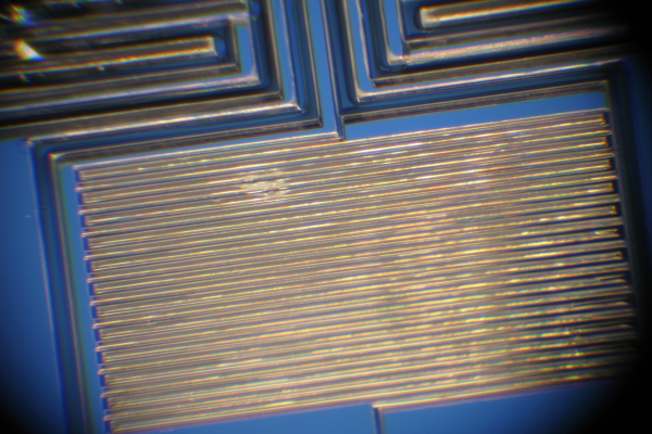
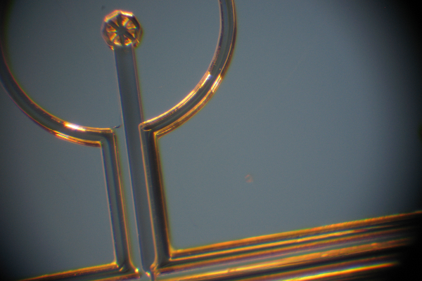
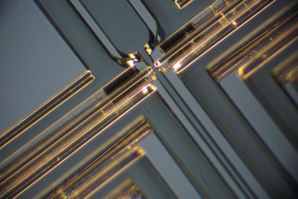
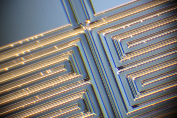
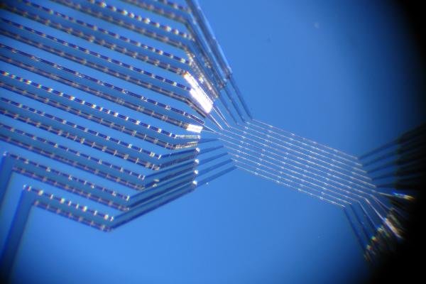
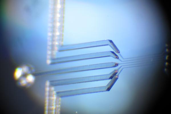
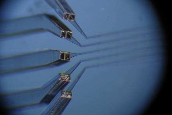
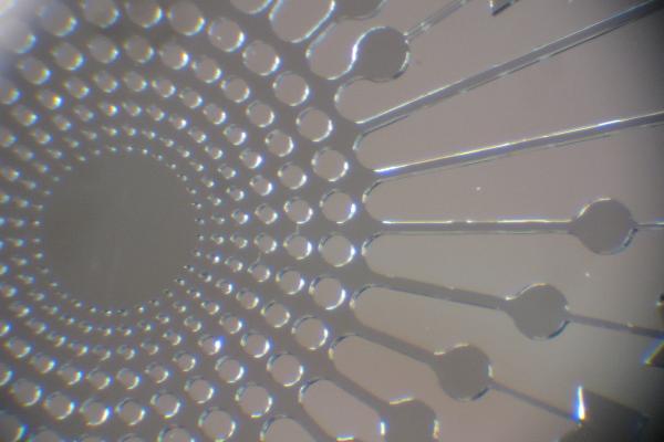
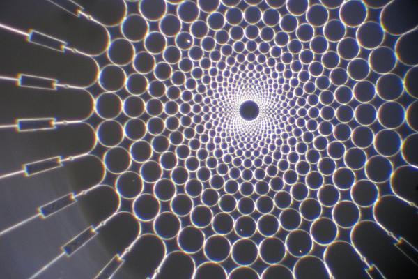
Lithography is the prerequisite for creating ordered structures as templates for two- or three-dimensional cavities in the range of sub-micrometers up to several hundred micrometers for cell experiments. Irradiation with UV light (photolithography) or accelerated electrons (electron beam lithography) triggers a photochemical reaction in photosensitive polymers. The reaction causes a change in the solubility of the polymer in corresponding developers, so that defined polymer structures are created on the wafer, which serve as masking for subsequent process steps such as etching or deposition of metallic films. We are also equipped to fabricate photomasks for shadow impact lithopgraphy by laser lithography.
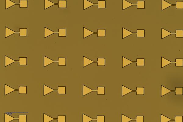
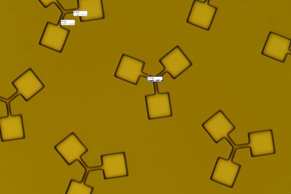
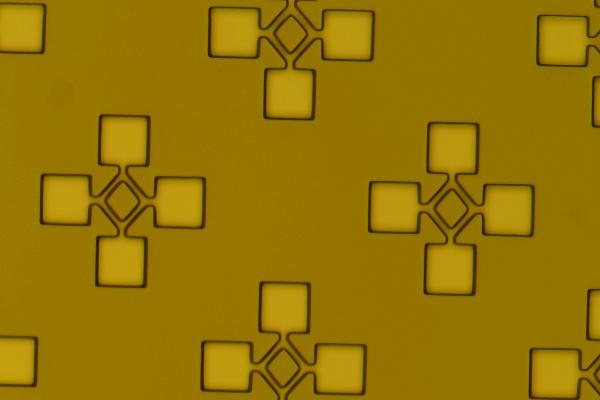
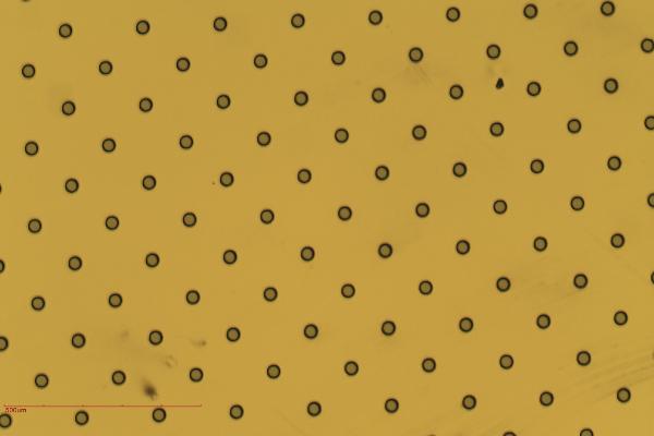
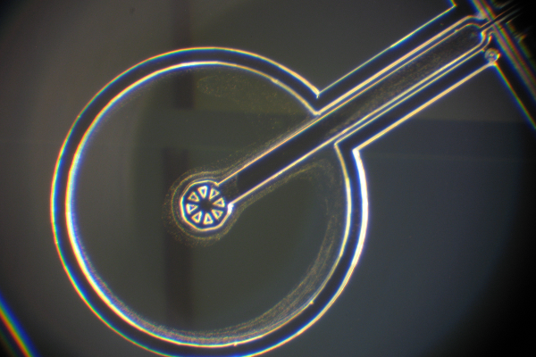
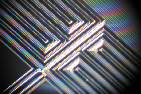
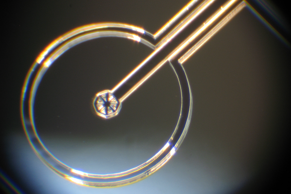
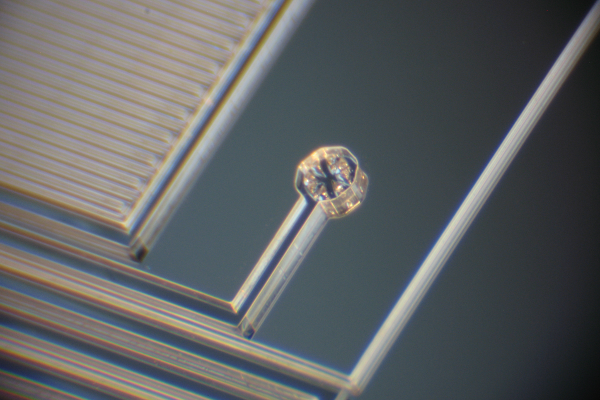
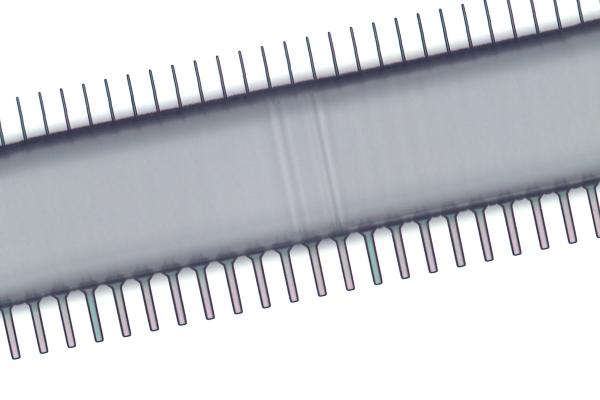
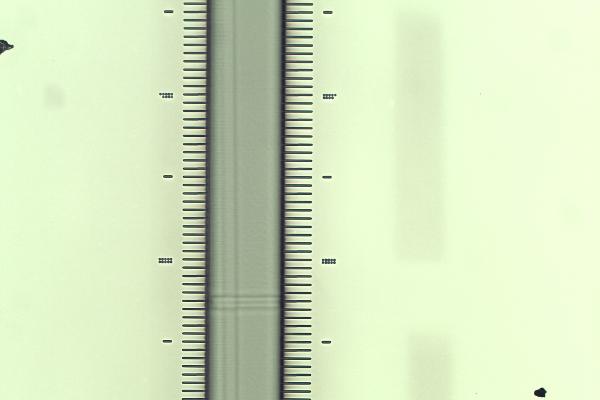
Optical microscopy image of a photolithographically produced Si master.
Optical microscopy image of a photolithographically produced Si master.
Optical microscopy image of a photolithographically produced Si master.
Optical microscopy image of a photolithographically produced Si master.
Optical microscopy image of a photolithographically produced Si master.
Optical microscopy image of a photolithographically produced Si master.
Optical microscopy image of a photolithographically produced Si master.
Optical microscopy image of a photolithographically produced Si master.
Optical microscopy image of a photolithographically produced Si master.
Optical microscopy image of a photolithographically produced Si master.
Optical microscopy image of a photolithographically produced Si master.
Rie Master
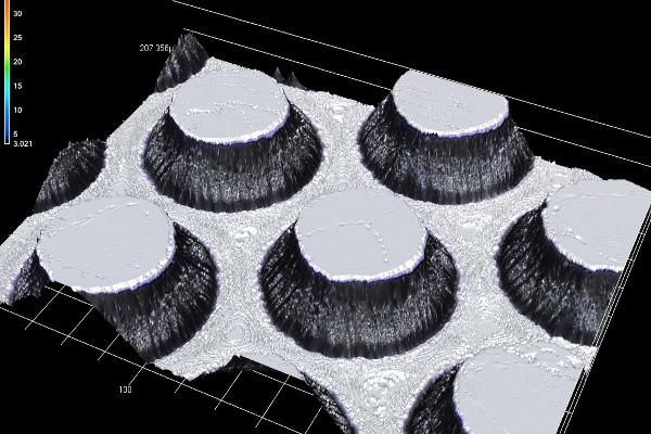
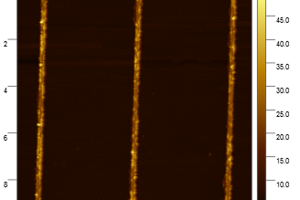
Suitable masters for the hot embossing process consist of mechanically and thermally resistant materials such as silicon or glass. Fluorine-based plasma etching processes such as reactive ion etching (RIE) can be utilized to successfully etch these structures into the materials mentioned. Here, the roughness of the etched surfaces and the edge angle of the structures can be adjusted by setting the etching parameters. These properties of the master have a great influence on the behavior of cells in the microwells thus created.
3d-Profile of a ICP-RIE etched Si-Master, used for thermal imprint
AFM-mesurement of a ICP-RIE etched Si-Master, used for thermal imprint
Electroplating
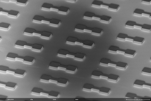
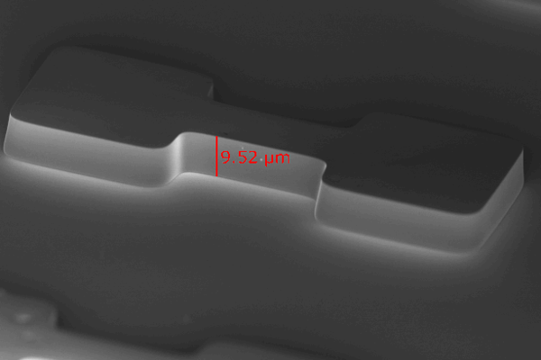
In contrast to (subtractive) etching of material, structures can be filled by coating processes (additive). Since microstructures are most important for our cell experiments, it is necessary that the deposition rate is relatively high and homogeneous over a large area. One method suitable for this purpose is the electrochemical deposition of nickel layers from an electrolyte in a process known as micro-electroplating. The structures grown in this way show a high mechanical stability and adhesion, so that such masters are just as suitable for the hot embossing process as those etched in silicon or glass. The biggest advantage of this method over most etching processes is that nearly perpendicular edges of the structures can be created without any problems, as long as the preceding lithography process is optimized accordingly.
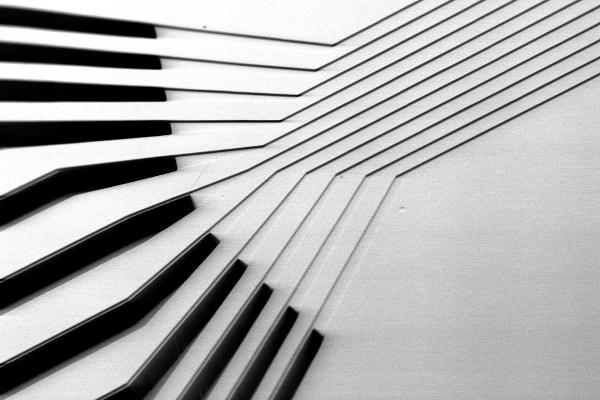
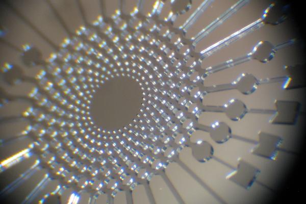
SEM image of an electroplated nickel master.
SEM image of an electroplated nickel master.
SEM image of an electroplated nickel master.
SEM image of an electroplated nickel master.
SEM image of an electroplated nickel master.
Microfluidics
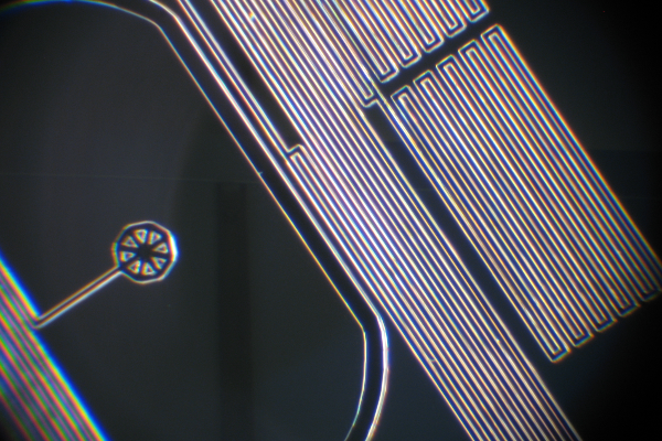
The term microfluidics covers methods that deal with the rapid and efficient manipulation of small quantities of fluids (µL or below). For example, our research uses microfluidic structures to mix liquids or to generate well-defined, identically sized droplets (oil / water). The chips are designed from scratch and manufactured by ourselves. Usually these fluidic structures are made of silicone, which are bonded to glass substrates for a perfect sealing. The control of these systems is software based and uses high precision flow meters.
Two step Lithography SU-8 Master designed for Microfluidics.
Two step Lithography SU-8 Master designed for Microfluidics.
Two step Lithography SU-8 Master designed for Microfluidics.

